")


Meta just unveiled four generations of custom silicon in a single announcement. The specs are striking. The strategy behind them is more interesting.
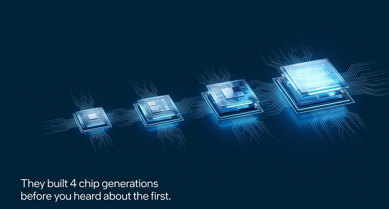
On March 11, 2026, Meta dropped what amounts to a two-year chip roadmap in a single blog post: four generations of its Meta Training and Inference Accelerator, announced together, spanning chips already in production to chips headed for mass production in early 2027. The MTIA 300 is live and running recommendation and ranking workloads right now. The MTIA 500 will deliver 30 petaFLOPS of MX4 compute and 27.6 TB/s of HBM bandwidth when it arrives.
That’s a 25x compute increase over the MTIA 300 across the product line. In under two years.
The announcement raises questions that go well beyond chip specs. Can Meta actually sustain a six-month silicon release cadence? Does this pressure Nvidia in any meaningful way? And what does it mean for the broader enterprise AI market when a consumer tech company starts publishing chip roadmaps that rival semiconductor incumbents? This analysis examines the full picture: what the chips do, who they threaten, where the risks sit, and what decision-makers should do with this information.
The MTIA Roadmap: What Meta Actually Announced
Meta’s MTIA program launched in 2023 with a first-generation inference chip. The March 11 announcement was a different order of magnitude. Meta’s official statement described “four new generations” on a cadence of “every six months or less.” That’s not a product launch. That’s a manufacturing and design philosophy.
The four chips break down as follows, based on detailed specs published by Tom’s Hardware:
| Chip | FP8 FLOPS | MX4 FLOPS | HBM Bandwidth | HBM Capacity | TDP | Status |
|---|---|---|---|---|---|---|
| MTIA 300 | 1.2 PFLOPS | — | 6.1 TB/s | 216 GB | 800W | Deployed |
| MTIA 400 | 6 PFLOPS | 12 PFLOPS | 9.2 TB/s | 288 GB | 1200W | Lab-tested |
| MTIA 450 | 7 PFLOPS | 21 PFLOPS | 18.4 TB/s | 288 GB | 1400W | Early 2027 |
| MTIA 500 | 10 PFLOPS | 30 PFLOPS | 27.6 TB/s | 384–512 GB | 1700W | Early 2027 |
Three things jump out. First, the MX4 precision format delivers roughly 6x the throughput of FP16 per clock cycle, which is why the compute numbers look so different between precision tiers. Second, HBM bandwidth grows 4.5x from the MTIA 300 to the 500, tracking the memory wall problem that dominates inference performance. Third, each chip slots into the same Open Compute Project rack standard, enabling data center swaps without infrastructure rebuilds.
The manufacturing stack behind this: TSMC on 3nm process nodes, Broadcom handling compute and I/O chiplet design, CoWoS advanced packaging. This isn’t a skunkworks experiment anymore. Meta is running serious silicon engineering at scale.
Why the Six-Month Cadence Changes the Calculus
The semiconductor industry typically runs on 12-to-24-month product cycles. Nvidia’s H100 to B200 arc took years of engineering. Meta is claiming a six-month generation-over-generation cadence. Whether that’s sustainable long-term is an open question, but the structural reasons it’s possible are worth understanding.
Custom silicon designed for a narrow workload class is far simpler to iterate than a general-purpose GPU. Meta’s chips are inference-first by design. They don’t need to support every CUDA workload, every graphics pipeline, every compute primitive that Nvidia’s customers demand. Narrower scope means faster design cycles, faster tape-out, faster validation.
“We’ve developed a competitive strategy for MTIA by prioritizing rapid, iterative development, an inference-first focus, and frictionless adoption by building natively on industry standards.”
— Meta Platforms, official March 2026 statementThe modularity helps here too. Swapping chiplets within the same rack-scale architecture means Meta doesn’t need to redesign the whole data center each generation. The 72-chip-per-rack MTIA 400 configuration reported by Yahoo Finance gives a sense of the density they’re targeting. New chips drop in. The surrounding infrastructure stays.
Meta is already operating at “hundreds of thousands” of MTIA chips for inference workloads, covering ad ranking, content recommendations, and organic feed algorithms. This isn’t a pilot program. The chips are carrying real production load across billions of daily users. That scale provides a feedback loop that no commercial silicon vendor can match for Meta’s specific workloads.
The Nvidia Rivalry: Competitive or Complementary?
Meta’s announcement landed as a direct competitive shot at Nvidia and AMD. Yahoo Finance coverage noted Meta’s claim that the MTIA 400 is “its inaugural chip that offers both cost efficiency and raw performance that competes with leading commercial products.” That’s a pointed benchmark assertion.
But the full picture is more nuanced. Meta is simultaneously a major Nvidia customer, and Mark Zuckerberg has made no secret of that relationship. The MTIA program isn’t a wholesale replacement strategy. It’s a diversification play targeting specific inference workloads where Meta has enough volume and predictability to engineer a purpose-built solution that beats general-purpose GPUs on cost per operation.
The efficiency claim is significant: analysis from AInvest puts MTIA’s gains at up to 7x for key matrix operations versus general-purpose silicon. For a company running inference at Meta’s scale, that efficiency gap translates directly to billions in infrastructure savings annually.
“The goal is clear: break the AI compute cost curve, aiming for up to 7x gains for key matrix operations.”
— AInvest, Meta MTIA cost analysis, March 2026For Nvidia, the real concern isn’t Meta. It’s what Meta’s success signals to every other hyperscaler. Google has TPUs. Amazon has Trainium and Inferentia. Apple runs Neural Engines. Microsoft has invested in Maia. Meta’s roadmap is the clearest evidence yet that custom silicon for AI inference is viable at production scale, not just a research exercise. That’s a structural shift in the competitive landscape, even if no single company is abandoning Nvidia GPUs tomorrow.
Technical Architecture: What Makes MTIA Different
MTIA’s inference-first design philosophy produces some specific architectural decisions worth examining for technically-oriented readers.
The MX4 precision format is central to the compute story. MX4 (Microscaling 4-bit) enables roughly 6x the floating-point operations per second versus FP16 at the same clock and power budget. This matters enormously for inference, where you’re running a trained model forward repeatedly at scale, not doing the high-precision arithmetic that training requires. Most inference workloads tolerate the precision reduction. The throughput gains are substantial.
FlashAttention hardware acceleration is built directly into the silicon. For transformer-based models (which now power most of Meta’s AI applications, from content ranking to Llama variants), attention computation is a primary bottleneck. Hardwiring it into the chip rather than implementing it in software on a general-purpose GPU is a meaningful advantage for Meta’s specific workload mix.
The software stack deserves attention. TrendForce reporting confirms native support for PyTorch, vLLM, and Triton, the dominant frameworks in Meta’s (and most of the industry’s) ML toolchain. Teams don’t need to rewrite models or change workflows to run on MTIA. This is the “frictionless adoption” Meta refers to, and it’s not a small detail. The biggest failure mode for custom silicon programs has historically been software ecosystem fragility.
The Data Center Dynamics writeup on the announcement confirms that by 2027, MTIA is targeting full generative AI workloads, not just ranking and recommendation. That’s a significant expansion of scope. Whether the architecture can handle GenAI inference at the scale Meta needs it to remains one of the key unanswered questions.
Risks and Honest Uncertainties
The announcement deserves scrutiny alongside the excitement. Several risk factors are real and worth naming directly.
Where the Skeptics Have a Point
- 3nm yields are hard. TSMC’s 3nm process is advanced but not without yield challenges. Meta’s cost projections depend on yields at scale that haven’t been publicly validated. TrendForce notes the manufacturing dependency without quantifying the risk.
- Development costs are real. Bloomberg reports Meta has spent millions on this program. The ROI case is built on scale that only a handful of companies globally can match.
- The six-month cadence is untested at this scope. Claiming it and executing it across four generations while managing yield, packaging, and software integration simultaneously is operationally demanding.
- Scope creep risk. Expanding from ranking/recommendation to full GenAI inference means more complex workloads with less predictable access patterns. MTIA’s architecture may face surprises.
- No independent benchmarks. All performance comparisons to Nvidia and AMD are Meta’s own assertions. Third-party validation at production scale hasn’t been published.
Meta’s $115 to 135 billion 2026 capex commitment, reported by TrendForce, gives the program a financial buffer that smaller organizations can’t replicate. But it also means the stakes on execution are enormous. A sustained yield problem or software integration failure on MTIA 450 or 500 doesn’t just affect a product line. It affects a quarter of a trillion dollars in planned infrastructure.
A Decision Framework for Enterprise Leaders
Most organizations reading this won’t be designing custom silicon. But this announcement has direct implications for infrastructure decisions being made right now.
Questions to Ask Before Your Next GPU Procurement
- What’s your inference-to-training ratio? If you’re running more inference than training (most production AI teams are), the efficiency argument for inference-optimized silicon is directly relevant to your cost model.
- Are your workloads predictable enough for custom silicon? MTIA works because Meta’s ranking and recommendation workloads are stable and high-volume. Diverse or experimental workloads still favor general-purpose GPUs.
- Do you have the volume to justify it? The economics of custom silicon require scale. For most enterprises, the relevant action is negotiating harder on Nvidia and AMD pricing, not designing chips.
- What’s your dependency concentration? If your AI infrastructure is 90%+ Nvidia, this announcement is evidence that diversification is both feasible and strategically important, even if you use commercial alternatives rather than custom silicon.
- Can your software stack absorb a hardware swap? Meta’s PyTorch-native approach lowers switching costs dramatically. If your team is framework-agnostic, inference hardware alternatives (Google TPUs, Amazon Inferentia) deserve fresh evaluation against your current Nvidia contracts.
What This Signals for AI Infrastructure Through 2027
The pattern emerging from this announcement isn’t just about Meta MTIA chips. It’s about a fundamental restructuring of how AI compute gets built and procured.
We’re moving from a world where “AI infrastructure” meant “buy Nvidia GPUs” to a world where the compute layer is fragmenting. Custom silicon programs at Google, Amazon, Microsoft, and now Meta are all heading in the same direction: inference workloads, which represent the majority of production AI compute by volume, are increasingly handled by purpose-built accelerators rather than general-purpose GPUs. Training still depends on Nvidia for most organizations, but inference is becoming a contested market.
For investors, the implications for Nvidia’s margins are worth watching. Nvidia’s dominance has historically come from a combination of hardware performance and CUDA ecosystem lock-in. Meta’s PyTorch-native approach for MTIA, and Google’s JAX stack for TPUs, are both evidence that the software moat is more crossable than it looked three years ago. Pressure on inference revenue could emerge as these programs mature.
Watch for three developments in the next 18 months. First, independent benchmarks comparing MTIA 400 to H100 and B200 on real inference workloads. Meta’s internal numbers will eventually face external validation or scrutiny. Second, whether the MTIA 450 and 500 timelines hold, specifically whether the six-month cadence survives the complexity jump to full GenAI workloads. Third, whether any other hyperscalers accelerate their own custom silicon announcements in response.
Meta has published a roadmap. Now comes the harder part: executing it.