Tesla Tapes Out AI5 Chip: Why Custom Silicon Is About to Change Edge AI Deployment Forever
The headline says “faster FSD.” The real story is a vertically integrated inference platform targeting NVIDIA’s edge dominance, at a fraction of the cost, embedded in millions of cars and robots.
The Story Nobody Is Actually Telling
On April 15, 2026, Elon Musk posted a photo of a silicon wafer and declared that Tesla’s next-generation AI5 processor had successfully taped out, chip industry shorthand for completing the physical design and sending it to a foundry. Within hours, every tech outlet ran a version of the same story: “Tesla’s new chip is 40× faster.” That framing is misleading. And the actual story is considerably more consequential.
AI5 is not primarily an upgrade for your Model Y. Musk confirmed that AI4 already achieves “much better than human safety” for Full Self-Driving, which means the compute bottleneck for vehicles is largely solved. AI5 is engineered for two different missions: powering Optimus humanoid robots with real-time edge inference, and scaling Tesla’s supercomputer training clusters. The car is almost incidental.
The deeper story is competitive strategy. By designing custom ASICs optimized for its own neural network architectures, Tesla can undercut NVIDIA’s edge inference economics by roughly 10× on cost and 3× on performance per watt. Multiply that across a fleet of millions of vehicles and robots and the result is a distributed AI inference platform of unprecedented scale, one that could eventually be offered to xAI, or used as a licensing wedge into the broader embodied AI market.
What Actually Happened on April 15
Tape-out is a hard milestone. It means the design is frozen, masks are cut, and fabrication begins. Engineering samples are now expected in late 2026, with volume production tracking for mid-2027. Musk simultaneously confirmed that AI6 and Dojo 3 are already in development, with AI6 tape-out expected December 2026.
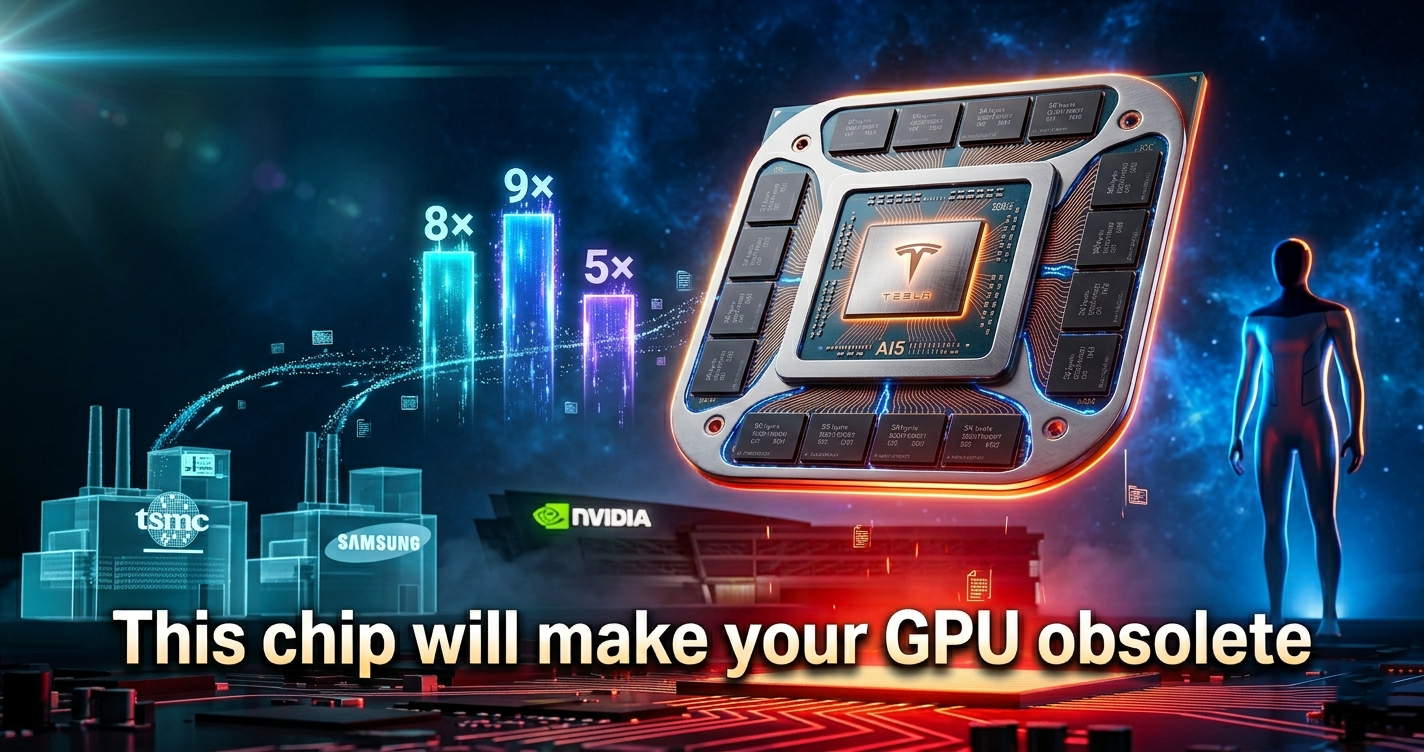
The performance claims are striking but require context. A single AI5 delivers 8× the raw compute of AI4, 9× the memory capacity, and 5× the memory bandwidth. The “40×” figure applies to targeted workloads, it bundles compute, memory bandwidth, and specialized accelerators into a composite metric. It is not a uniform speedup across all tasks. No independent lab has benchmarked a physical sample yet, because none exist.
Tesla is dual-sourcing production across TSMC and Samsung, a supply-chain hedge that signals how seriously the company treats AI5’s volume ambitions. That accidental mention of “TSC” in early coverage (later corrected) points to TSMC’s N3 process node, the same advanced node Apple uses for M-series chips. Samsung’s Taylor, Texas fab handles a parallel production stream, though yield issues at the Taylor facility contributed to AI5 slipping nearly two years behind its original H2 2025 schedule.
“AI5 will be 40 times better than AI4 by some metrics… we work so closely at the hardware-software level.”
— Elon Musk, X, April 15, 2026
Architecture: What Tesla Actually Built
The design decisions inside AI5 are as revealing as the headline numbers. Tesla removed the legacy GPU and Image Signal Processor (ISP) that occupied significant die area in AI4, replacing them entirely with Tesla-specific neural network accelerators, Arm CPU cores, and PCI interface blocks. Every transistor serves Tesla’s own model architecture. Nothing is there for general-purpose compatibility.
The memory subsystem is similarly opinionated. Twelve SK Hynix memory packages surround the die on a ~384-bit interface, likely GDDR6 or GDDR7 rather than HBM. Tesla engineers debated HBM’s higher bandwidth ceiling but chose conventional GDDR for its cost and manufacturability advantages at scale. For Optimus robot deployments, where cost per unit is critical, that tradeoff makes sense. For pure training throughput, it limits ceiling performance.
| Specification | AI4 | AI5 | Delta |
|---|---|---|---|
| Raw compute | Baseline | 8× AI4 | +700% |
| Memory capacity | Baseline | 9× AI4 | +800% |
| Memory bandwidth | Baseline | 5× AI4 | +400% |
| Memory interface | — | ~384-bit GDDR6/7 | — |
| Peak power | ~300W | Up to 800W | ~2.7× |
| Target (robot) power | — | ~250W | — |
| Useful compute (vs dual AI4) | 1× | ~5× | +400% |
The power story deserves attention. The chip targets 250W for Optimus use but reaches 800W peak , nearly three times the thermal envelope that HW4 vehicle liquid cooling was designed for. That gap explains why AI5 requires a different board layout and connector type, making it incompatible with existing HW4 vehicles. Owners waiting for a retrofit will be waiting a long time.
The Competitive Stakes for NVIDIA and Everyone Else
The frame that matters for ML engineers and CTOs is cost-per-inference, not raw FLOPS. A single AI5 reportedly approaches NVIDIA Hopper (H100) inference throughput at 150–250W versus the H100’s 700W. Dual AI5 configurations are projected to match Blackwell (B200) performance at a fraction of the per-unit hardware cost. These claims require independent verification, but if they hold under real workloads, the economics of running inference at the edge shift dramatically.
NVIDIA’s edge AI margin depends on nobody having a better alternative. Tesla is building one for itself. The risk for NVIDIA isn’t that Tesla starts selling chips, it almost certainly won’t. The risk is that Tesla’s success makes the case for other large-scale deployers to follow suit, accelerating the custom ASIC trend that Google (TPU), Amazon (Trainium/Inferentia), and Microsoft (Maia) are already executing in the cloud.
The edge AI hardware market is tracking from $26.14B in 2025 to an estimated $58.90B by 2030 (CAGR 17.6%), per MarketsandMarkets. Tesla’s AI5 enters this market not as a product for sale but as a moat, a reason every competitor must either match Tesla’s ASIC investment or absorb the NVIDIA premium Tesla no longer pays.
For robotics and autonomy startups, the benchmark has just been set publicly. Teams that were “planning to evaluate custom silicon later” now have a concrete performance target to beat. The “just use GPUs” default for robotics inference becomes harder to defend when a competitor is running at 10× lower cost per inference on proprietary hardware.
What This Means for ML Engineers Right Now
The critical gap in all current coverage: nobody has addressed what AI5 means for developer workflow. Tesla’s AI4 and earlier chips required model teams to work with Tesla’s internal compiler stack, with limited official SDK exposure for external researchers. AI5 removes both the traditional GPU and the ISP, components that many existing optimizations assumed were present.
No SDK release has been announced. Tesla’s internal teams likely already work against AI5 simulation environments, but external developers — including those building on FSD APIs or evaluating Tesla hardware for third-party robotics, are in the dark. Whether existing PyTorch or JAX pipelines require significant rewrites for AI5-specific quantization, operator fusion, or memory layout is unknown.
The architectural shift toward pure neural accelerators (no legacy GPU path) suggests that inference code relying on general CUDA-style parallelism will need reworking. Model compression strategies optimized for AI4’s memory hierarchy won’t transfer directly. Engineering teams that want to be ready when AI5 samples ship in late 2026 should start profiling their inference workloads against the published memory bandwidth figures now.
Reality Check: The Hype and the Hard Limits
✓ Confirmed
- Design locked, tape-out complete April 15
- Dual-foundry (TSMC + Samsung) confirmed
- AI4 sufficient for current FSD safety targets
- AI5 optimized for Optimus and supercomputers
- AI6 and Dojo 3 confirmed in development
⚠ Unverified
- “40×” performance: composite metric, no independent benchmarks
- 2027 production: already 2 years behind original promise
- Thermal targets: 800W peak vs. 250W goal is a wide gap
- Sensor suite remains the actual FSD ceiling, not compute
- AI6/Dojo 3 timelines: AI6 already slipped 6 months
The most pointed skeptical critique comes from Electrek’s Fred Lambert, who observed that “the pattern is hard to miss: Tesla keeps moving the goalpost to the next chip instead of delivering what was promised.” HW3 owners were told hardware upgrades were coming. They never arrived. HW4 owners will likely face the same calculus — AI5 requires new board architecture and thermal management that makes retrofitting existing vehicles uneconomical.
The automotive qualification timeline is real and rarely discussed. An anonymous silicon engineer with 20+ years of ASIC experience estimated that ISO 26262 functional safety certification alone adds approximately 18 months after silicon bring-up. Even on an aggressive schedule, AI5 in production vehicles arrives no earlier than late 2028. Robots face a different certification path but their own integration challenges.
Action Items by Audience
ML & Software Engineers
- Profile current inference workloads against AI5’s published bandwidth specs (5× AI4, ~1.3–1.5 TB/s est.)
- Audit PyTorch/JAX model code for GPU-specific paths that assume legacy rasterization or ISP preprocessing
- Follow Tesla AI’s GitHub and developer channels — SDK announcements will land before hardware samples
- Begin quantization experiments targeting architectures without dedicated ISP pipelines
CTOs & Tech Leaders
- Reassess robotics pilot hardware budgets: if Tesla AI5 specs hold, NVIDIA edge GPUs may carry a 10× cost premium by 2027
- Model a “custom ASIC” scenario in your 2028 infrastructure plan, Tesla’s move accelerates the timeline for all edge AI verticals
- Flag HW3/HW4 fleet upgrade risk for Tesla vehicle fleets, AI5 is board-incompatible, no retrofit path announced
- Evaluate xAI / Dojo partnership signals as a potential licensing channel for AI5-derived compute
Frequently Asked Questions
The Bottom Line
Tesla’s AI5 tape-out is a genuine engineering milestone, not a vaporware announcement. The design is locked, foundry partners are committed, and the architecture makes clear strategic sense: strip out every general-purpose component, optimize every transistor for Tesla’s own inference workloads, and manufacture at a scale that makes unit economics unbeatable. The 54% U.S. EV market share Tesla held in Q1 2026 means AI5 enters volume deployment into a fleet that no competitor can match in size.
What the next 18 months will determine: whether Samsung Taylor’s yield stabilizes fast enough to hit the mid-2027 production target; whether Tesla publishes developer tooling that lets external teams optimize for AI5’s architecture; and whether the chip’s thermal profile can be tamed to 250W in Optimus’s constrained form factor. Each of those is genuinely uncertain. The 40× headline and the stock-price pop are noise. The structural shift, Tesla operating as a vertically integrated silicon company competing at the inference layer against NVIDIA, is the durable signal. Watch the SDK announcement, not the wafer photo.
SIMPLY GREAT